
Palo Alto/Bhubaneshwar-TNI Bureau: In a momentous development for the state of Odisha, global chip design leader Synopsys has announced its plans to set up a design-centered facility in Bhubaneswar. Synopsys, renowned for its presence in over 25 countries and expertise in Electronics Design and Automation (EDA), is poised to strengthen Odisha’s semiconductor ecosystem with the establishment of this new center.
The facility, which will gradually expand to accommodate 300 chip design engineers, will house top teams from Synopsys, including Hardware Analytics and Test (HAT) and Hardware Development Group (HDG), including HDG Analog and HDG Design/Verification.
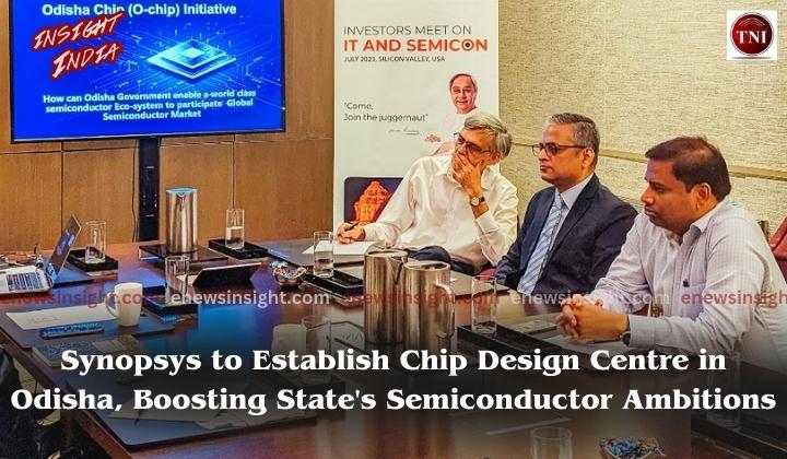
The announcement came after a crucial meeting between the company’s senior executives and a delegation from the Odisha government. During the meeting, the delegation emphasized the state’s commitment to building a resilient semiconductor ecosystem and highlighted the Semiconductor Manufacturing and Fabless Policy, which has received Cabinet approval. The policy offers generous incentives to both fab and fabless units and is part of the state’s initiative to foster a conducive environment for semiconductor research and development.
One of the key initiatives discussed was the upcoming O-Chip program, which aims to provide design infrastructure and training support to researchers, startups, and companies. The program has a visionary goal of establishing a next-generation Silicon Valley in Odisha and focuses on empowering talent and industry expertise, forging research partnerships, and attracting semiconductor companies.
Impressed by the government’s efforts, the Synopsys leadership pledged their full support to Odisha’s semiconductor ambitions and formally announced their plan to set up the chip design centre in the state. This move is expected to significantly boost the state’s readiness in the semiconductor industry and facilitate industry collaborations, internships, and research partnerships.
To ensure the success of the O-Chip program and provide the best advisory and mentorship support, the delegation engaged in extensive interactions with prominent industry leaders and researchers based in Silicon Valley. These industry veterans offered to come onboard as advisors and mentors, providing invaluable guidance to the initiative and encouraging active participation from semiconductor companies, universities, and experts.
In a separate event, the delegation also addressed the Odia diaspora, praising them for their continued support in preserving the socio-cultural ties with their homeland. The event witnessed the participation of over 900 people of Odisha origin and was organized by the Tourism Department in association with FICCI.
The delegation’s visit to Silicon Valley has been highly successful, with several global IT, electronics, semiconductor, and AI/ML companies announcing their plans to set up operations in Odisha. With strong government support and a surge in investment activity, the state is creating more employment opportunities for its people and emerging as a significant player in the semiconductor industry.
The establishment of the Synopsys chip design center marks a crucial milestone in Odisha’s journey towards becoming a global hub for chip design and semiconductor research, propelling the state’s technological growth and prosperity.


